
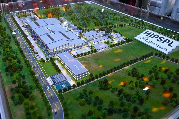

Bhubaneswar, May 29: A landmark Memorandum of Understanding (MoU) has been signed between the Government of Odisha, Intel Corporation, and US-based 3DGS Inc. to establish India’s first advanced packaging glass core substrate manufacturing facility in the Bhubaneswar–Khurda region. The project involves an investment of nearly USD 3.3 billion (₹27,500 crore) and is expected to generate over 1,800 direct high-skilled jobs.
The facility will focus on substrate manufacturing technology, a critical component in next-generation semiconductor devices. The project will be implemented in phases over the next 5–6 years, with technology transfer and skill development forming a key part of the initiative.
Officials highlighted that the MoU marks a major step in strengthening India’s semiconductor ecosystem, aligning with the Government of India’s vision to build a complete domestic manufacturing chain. The Odisha project complements ongoing semiconductor initiatives in Gujarat and Assam, positioning India as a global hub for advanced electronics.
The collaboration follows recent partnerships with Applied Materials, Lam Research, Tokyo Electron, Merck Electronics, and Tata Electronics’ tie-up with ASML, reflecting growing international confidence in India’s semiconductor roadmap.
Beyond direct employment, the project is expected to spur ancillary industries, logistics, and infrastructure growth in Odisha, while reducing India’s dependence on imports and enhancing its role in global supply chains.
State officials described the MoU as a transformative opportunity for Odisha, bringing high-tech manufacturing to the region and reinforcing India’s position in the global semiconductor landscape.